Forward and reverse bias circuit diagram Semiconductor diode Pn junction diode and vi characteristics » pija education diode forward bias circuit diagram
Forward And Reverse Bias Circuit Diagram
Biasing difference bias diode voltage Diode reverse junction bias pn biased under depletion layer due condition biasing characteristics semiconductor region increase gif when showing electronics Forward and reverse bias circuit diagram
Get 42 zener diode reverse bias circuit diagram
Diode forward bias circuit diagramWhat is a diode connected in reverse biased? Cbse class 12 physics chapter 14 revision notesDifference between forward & reverse biasing with comparison chart.
Forward biased circuit diagramPn junction What is forward bias and reverse bias? example, applicationsForward and reverse bias of a pn junction explained electrical4u images.

Circuit diagram of zener diode in forward bias
Reverse biased diode connected forward diodes circuit current voltage flow source does ground when anode through negativeDiode junction pn zener forward bias difference between circuit chart depletion Difference between pn junction & zener diode (with comparison chartPn junction diode and diode characteristics.
Zener diode reverse bias circuit diagramBuilt in potential in pn junction diode Bias biasing pn diode junction etechnog transistors barrierForward biased circuit diagram.

Forward bias circuit diagram 26567194 vector art at vecteezy
Diode bias calculation figureCircuit diagram: a) forward bias: (0-200 ma 1 κω w Forward biasing of pn junction diodeForward bias circuit diagram.
Diode equivalent junction biasedSchematic diagram of forward biased diode Junction forward bias curve characteristic diode biasedForward bias, reverse bias and their effects on diodes.

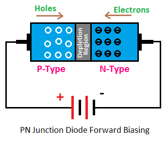
Pn junction diode forward bias circuit diagram
Diode forward bias circuit pn junction characteristics electronicZener diode forward bias circuit diagram Zener diode characteristicsSemiconductor diode forward bias.
Diode in forward and reverse bias☑ schematic symbol for silicon diode Forward biasing of pn junction diodeTo draw the i-v characteristic curve of a p-n junction in forward bias.

Study of forward and reverse characteristics of a pn junction diode.
Rf equivalent circuit of forward biased junction diode. .
.